Capabilities
The full spec sheet — no guesswork.
Honest tolerances, real materials and the equipment that backs them. If your design pushes a limit, talk to us before you redesign.
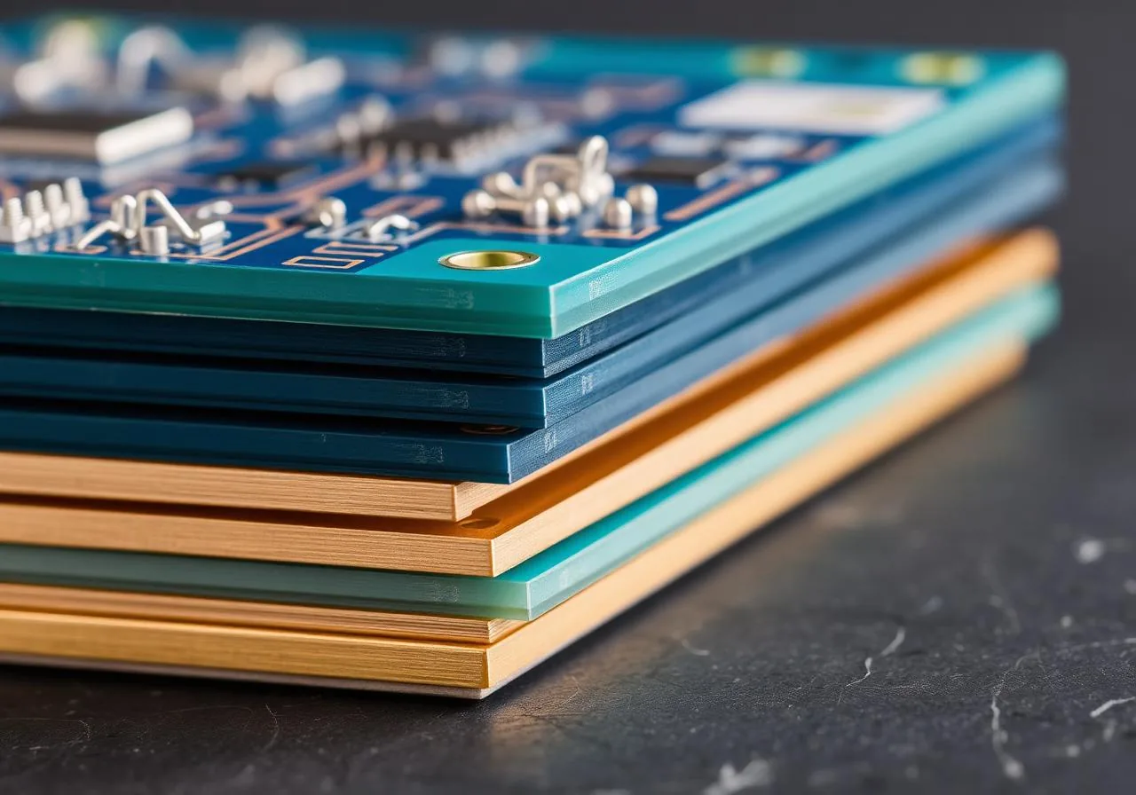
PCB Fabrication
- Layer count
- 1 – 32 layers
- Board thickness
- 0.2 mm – 6.0 mm
- Min trace / space
- 2.5 mil / 2.5 mil
- Min hole size
- 0.1 mm mechanical · 75 µm laser
- Aspect ratio
- Up to 12:1
- Copper weight
- 0.5 oz – 6 oz inner / outer
- Impedance control
- ±5% (single-ended & differential)
- Surface finish
- HASL · LF-HASL · ENIG · ENEPIG · OSP · Imm. Ag/Sn · Hard Gold
- Soldermask
- Green · Blue · Red · Black · White · Matte · Glossy
- Substrates
- FR-4 · High-Tg · Rogers · Polyimide · Aluminum · Ceramic
PCBA Assembly
- Component size
- 01005 (0.4×0.2 mm) and up
- BGA pitch
- Down to 0.3 mm · µBGA, CSP, QFN, LGA
- Board size
- 10×10 mm – 600×450 mm
- Process
- Lead-free · Leaded · Mixed · Press-fit
- SMT lines
- 8 high-speed lines, 2-shift capacity
- Throughput
- 120,000 placements / hr per line
- Test
- AOI · SPI · 3D X-ray · ICT · FCT · Burn-in
- Standards
- IPC-A-610 Class 2 & 3 · J-STD-001
- Cleaning
- Aqueous inline · No-clean compatible
- Conformal coating
- Acrylic · Silicone · Urethane · Parylene
Quality System
Certified at every step.
Our quality system is built around the standards your industry already requires — so you don't have to qualify us from scratch.
ISO 9001:2015
ISO 13485 Medical
IATF 16949 Auto
ISO 14001 Env.
UL Recognized
RoHS · REACH
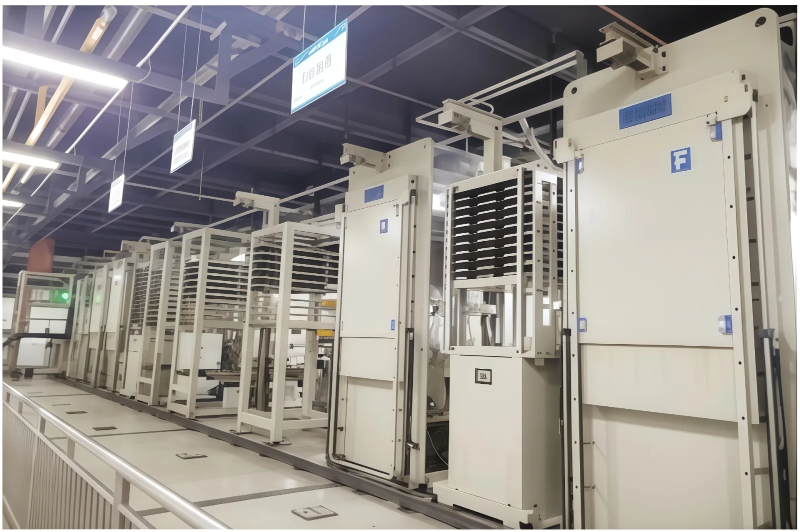
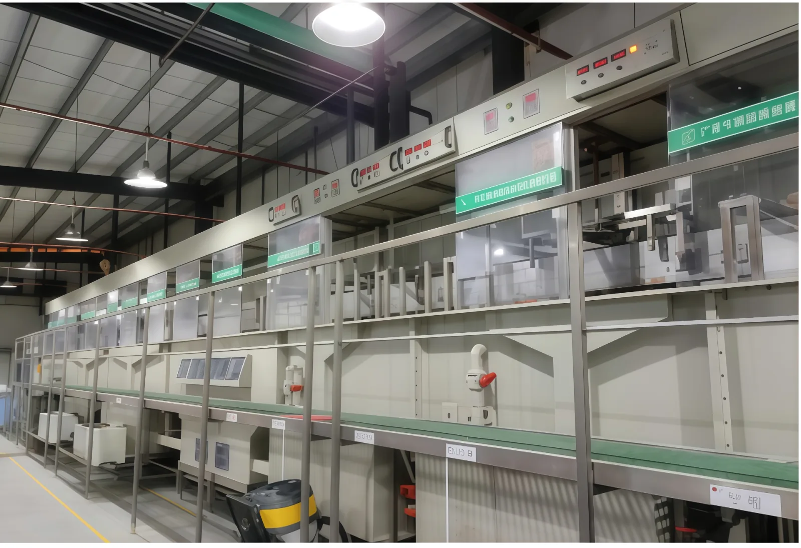
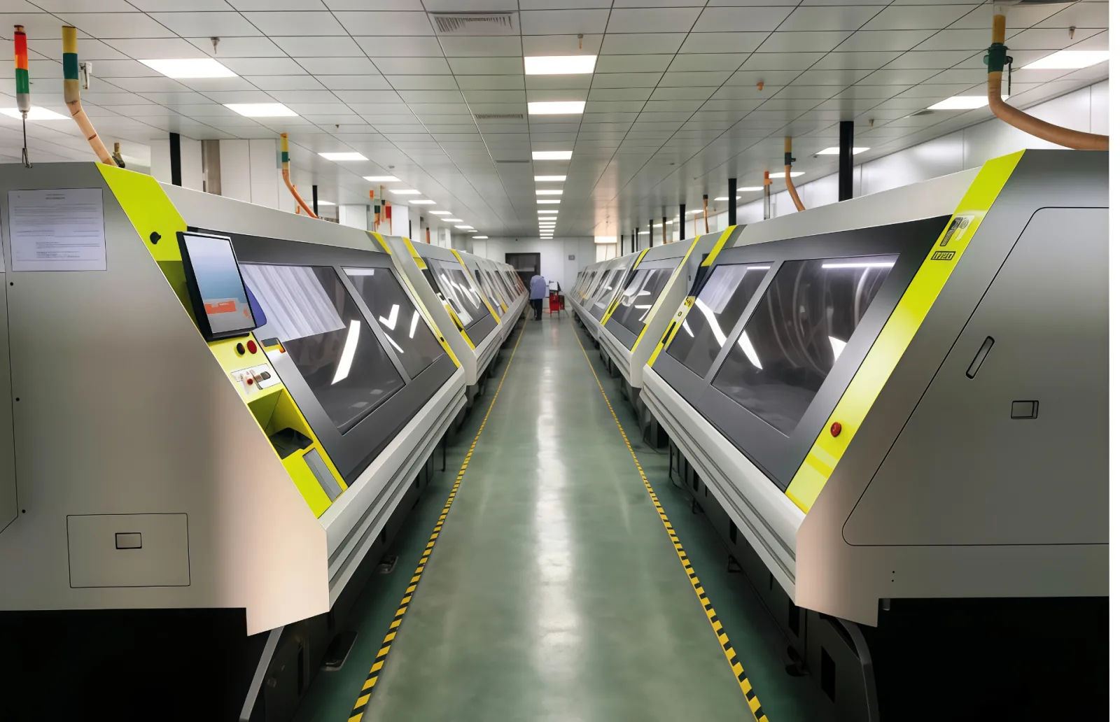
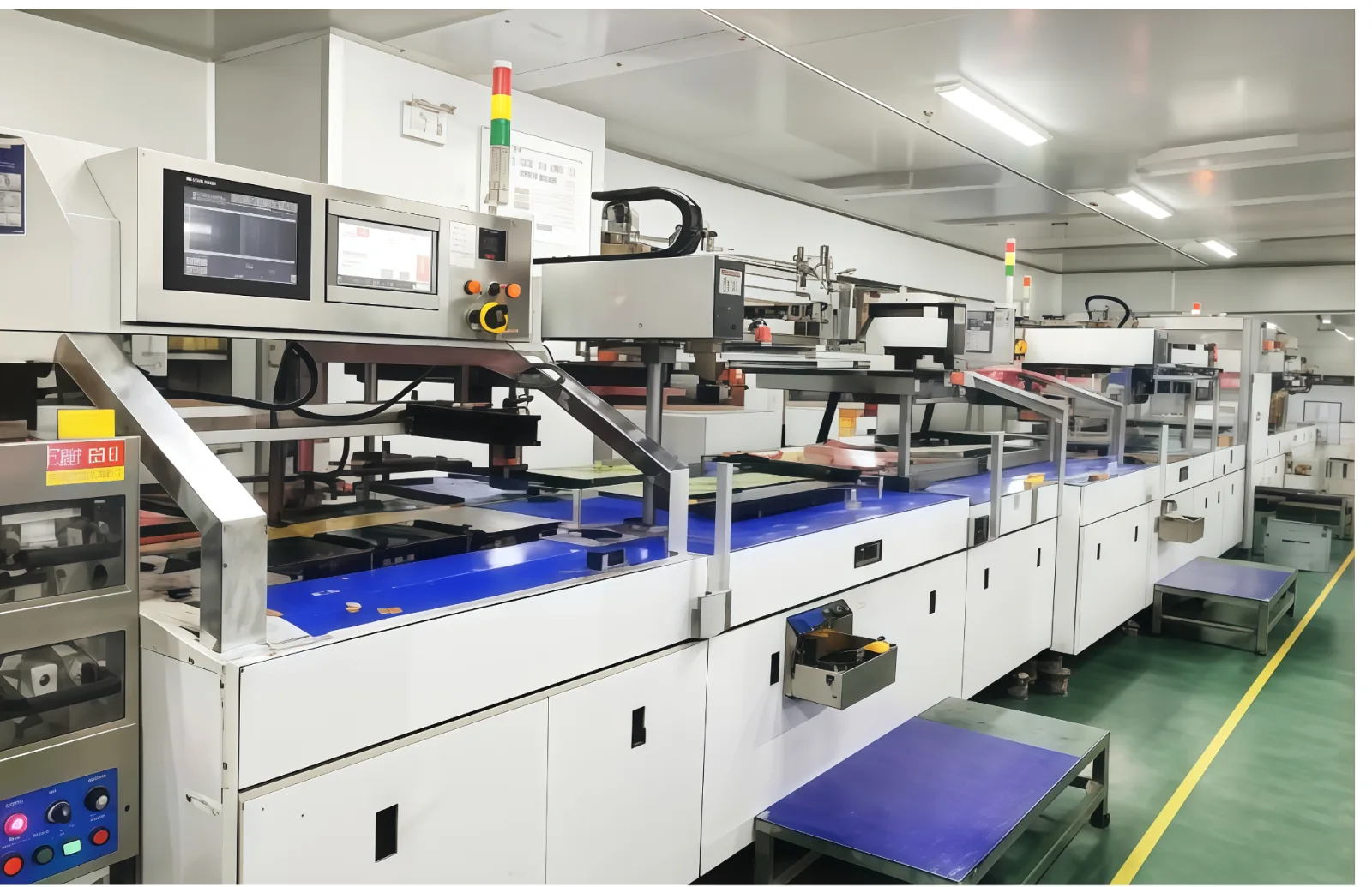
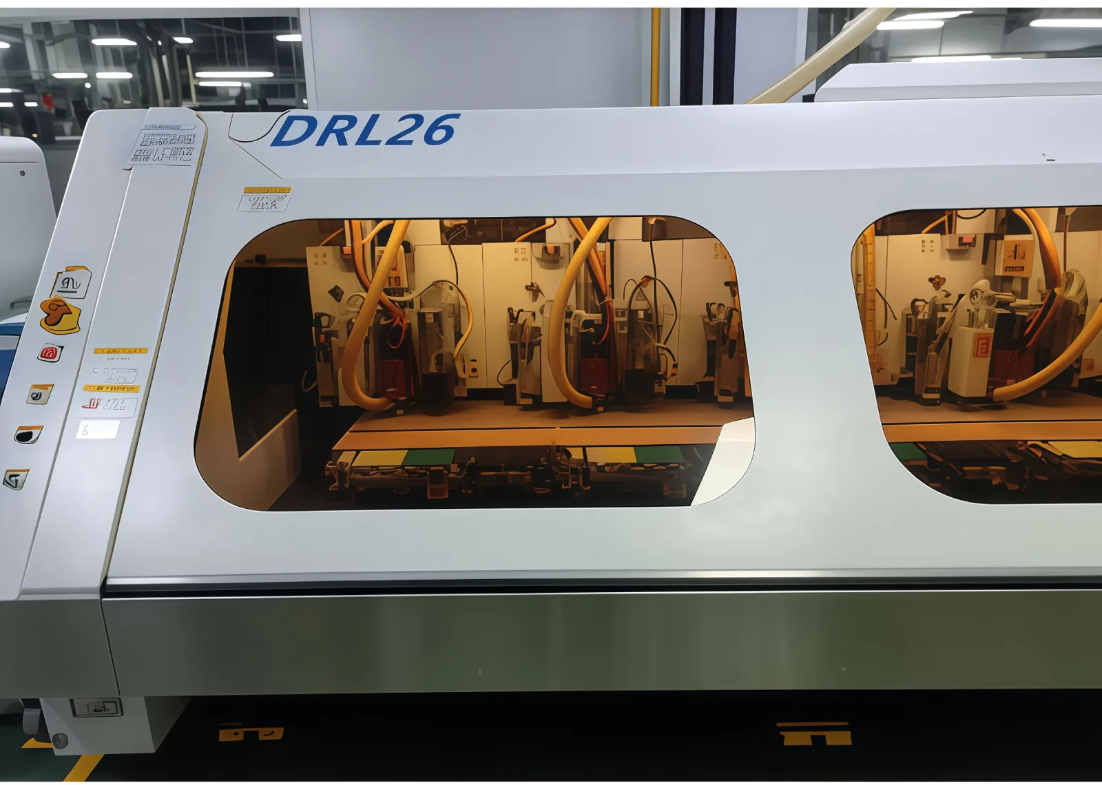
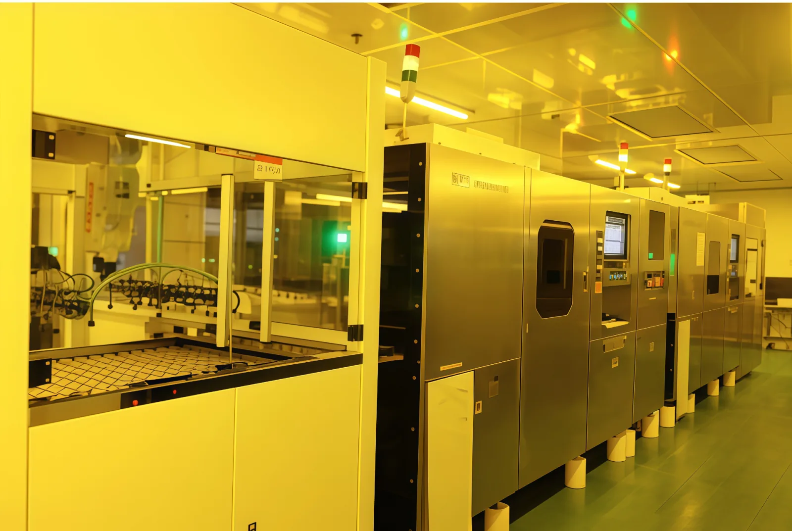
Inside the Factory
Production Equipment & Facility
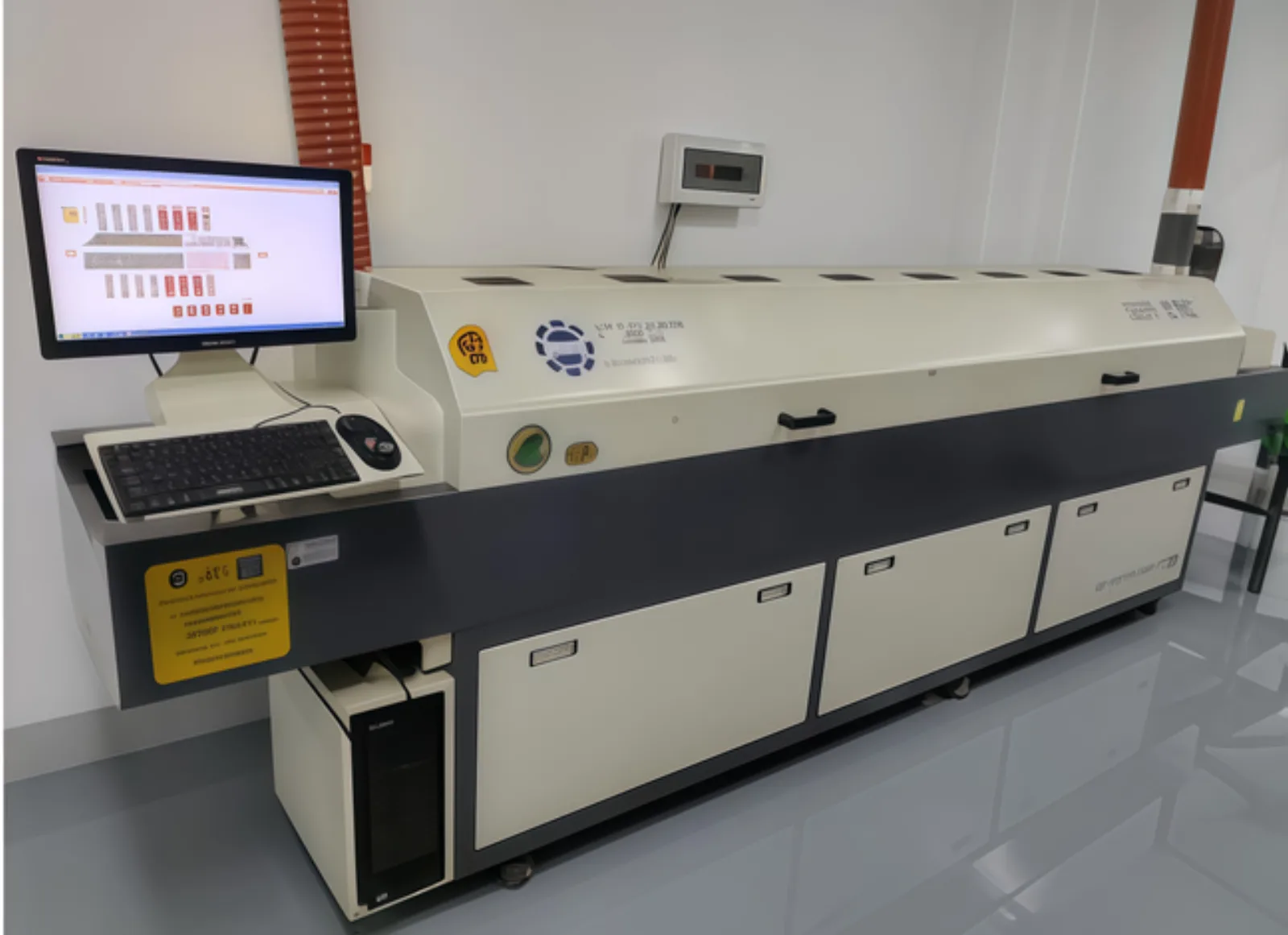
A look at our automated PCB manufacturing lines — precision plating, wet-process chemistry, and inline quality control engineered for consistent high-volume output.
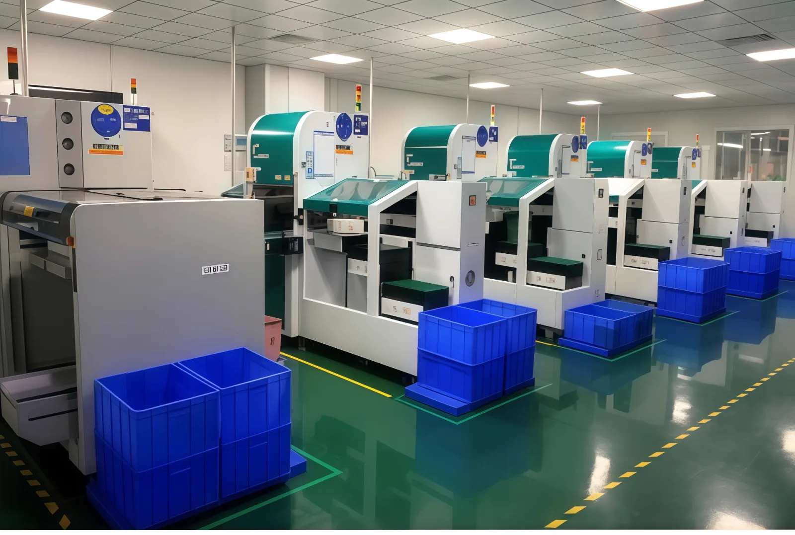
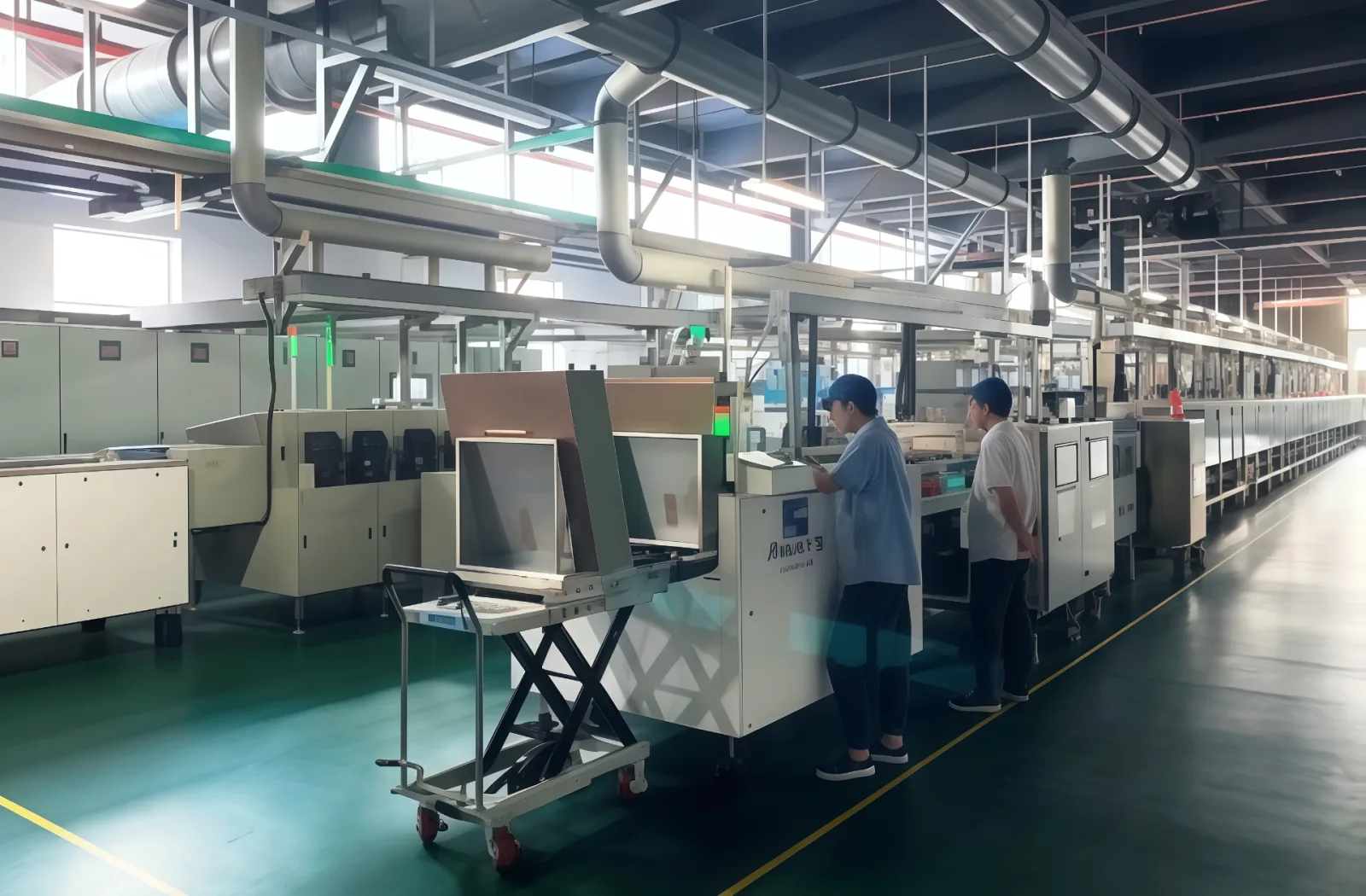
Quality & Testing
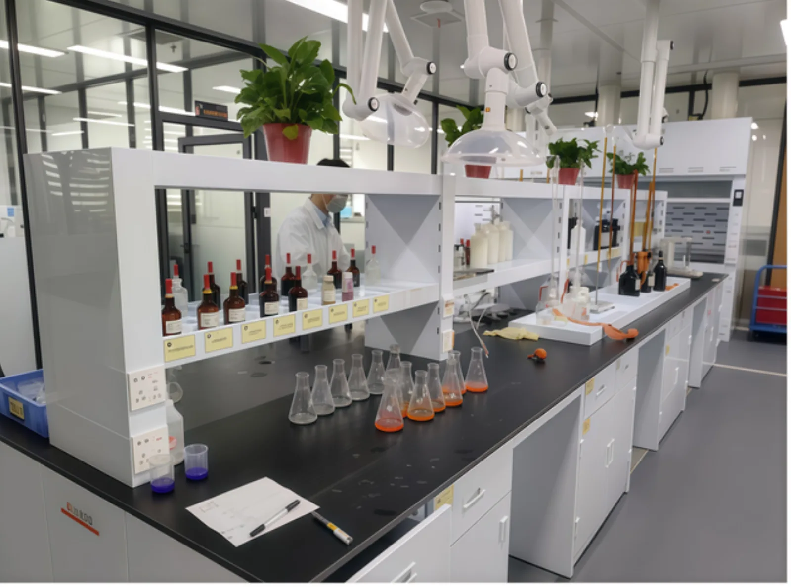
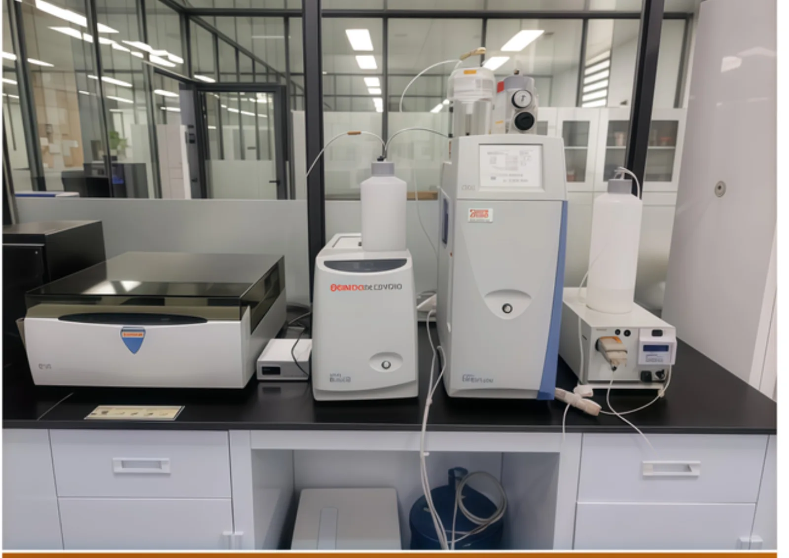
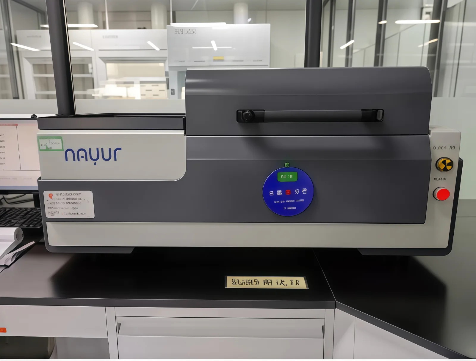
Inspection & Laboratory Equipment
Dedicated chemistry lab and metrology instruments — wet-chemical analysis, ion chromatography, reflow profiling and XRF coating measurement — ensure every board meets specification before it ships.